

|
|
|
|
|
|
|
|
|
 |
How do Avto Metals work? Broadly, Avto Metals are materials designed so that their emission of electrons can be regulated and their electrical properties thereby changed as desired. The science is similar to that used in theatres and concert halls to reduce echo effects.  Echo effects are caused by the reflection of sound waves from the theatre's walls.
In modern theatres and concert halls, patterns are built into the walls to reduce
echoes. By modifying the shape of the walls, the reflection of the sound waves can
be changed and echoes can be reduced or eliminated.
Echo effects are caused by the reflection of sound waves from the theatre's walls.
In modern theatres and concert halls, patterns are built into the walls to reduce
echoes. By modifying the shape of the walls, the reflection of the sound waves can
be changed and echoes can be reduced or eliminated.
The Avto Effect is the same principle, in this case altering the reflection of electrons from the surface of a material using the wave properties of the electrons. Until now, scientists have not exploited the wave properties of electrons because those properties become useful only when the dimensions of a structure reach nanoscales. It is well known in quantum mechanics that electrons have wave properties. But this knowledge has had no practical application because until now the dimensions of microelectronic components were too large to exploit electron wave properties. With today's achievements in nanoelectronics it becomes possible to fabricate objects having dimensions small enough to exploit the wave properties of electrons. Using the wave properties of electrons to alter the characteristics of a material makes it possible to fabricate new classes of devices. For example, smaller, cooler-operating, more-effective and less expensive diodes, transistors, and flat-panel displays can be built. In addition, more-powerful semiconductor lasers and more-sensitive infrared detectors will be possible. And there are many more potential applications. In all these devices, the work function of the material-the energy required to remove an electron from a solid material-defines its quality and complexity of production. The Avto Effect allows us to regulate precisely the work function of a material without changing its chemical composition. For example, the work function of a material such as silicon can be easily varied. The Avto Effect operates by modifying the geometry of the surface of the material in such a way that the wave properties of electrons become considerable. Understanding the Science For those interested, a full scientific explanation of the theory and methodology is available. But here is a brief explanation. Recent development of such technologies as electron beam milling and ion beam lithography enable the fabrication of structures with dimensions as small as a few nanometers. Those small dimensions are comparable to the de Broglie wavelength of a free electron inside the material. Because of this, it has become possible to fabricate some microelectronics devices working on the basis of the wave properties of electrons. When regular indents, influencing free electron de Broglie waves, are etched into the surface of a metal, the work function, and thus the electrical characteristics, of the metal can be changed. In the well-known case of a fermion inside a potential energy box, modification of the geometry of the boundary of the potential energy box will affect the boundary conditions for the particle wave function, and the resulting solutions for Schroedinger's equation. The behavior of fermions inside this potential energy box will be altered, and when the fermion is an electron and the potential energy box is a metal, modification of the metal's surface will lead to an increase of the Fermi energy level, with a resulting decrease in the work function of the metal. The wave properties of electrons inside a solid are well known and understood. There are some nanoelectronic devices, such as resonant tunneling diodes and super lattices, which utilize the wave properties of electrons. Under certain conditions electrons in the solid can be understood as a planar wave. Assume a solid with the surface geometry, as shown in Fig 1a, in which periodic indents are introduced in the flat surface of the solid. Let us consider an electron coming towards the border of the solid as planar wave 1. Wave 1 will reflect back from the border of the solid because the electron does not have enough energy to leave the solid. Because of the geometry of the surface there will be two reflected waves. One will reflect from the top of the indent (wave 3) and other will reflect from the bottom of the indent (wave 2). If the indent depth is one quarter of the de Broglie wavelength of the electron, waves 2 and 3 will interfere destructively and there will be no reflected wave. As a result, an electron of a certain energy cannot reflect back from the surface because of its wave nature. On the other hand, the electron cannot leave the solid and enter the vacuum because it does not have enough energy to overcome the potential barrier. For obvious reasons, the electron cannot simply stop near the surface either. From the quantum mechanical point of view, we can say that all possible final quantum states for that particular electron are forbidden. As all the final quantum states are forbidden, then the initial quantum state is also forbidden. 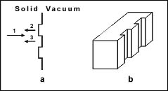 Figure 1: Wave interference diagram. As a result, the density of the quantum states inside the solid will be reduced. A 3D drawing of the solid is shown in Fig. 1b. Inside the solid there are standing de Broglie waves. Each standing wave corresponds to the quantum state which could be occupied by the free electron. The number of standing waves inside such a 3D structure is lower than in the case in which there were no indents and all the walls of the solid were plain. The end result of the ability to regulate electron wave properties is that the work function of a material can be reduced as desired and thus the electrical characteristics of the material can be changed at will. What will Avto Metals do? In principle, this technique can be applied to any metal, as well as some other materials such as glass, and it can be customized to allow for multiple band gaps and precise control of the electrical properties of the resulting materials. Copyright © 2006 - 2025 Avto Metals plc. All rights reserved. Forward Looking Statement may be found at http://www.avtometals.gi/fwdlook.shtml. |